Micro Vias Affect the Manufacturability of PCBs
Using micro vias in PCBs provides designers with a number of benefits including improving signal integrity, increasing space utilization, and providing long-term reliability. While these advantages are clear, there are also challenges with the design and fabrication of these structures that require careful attention. In this blog post, we will discuss how these challenges impact the manufacturability of a PCB and how to avoid them.
As technology continues to shrink, it becomes increasingly difficult to accommodate components and copper traces on a single circuit board. This is where micro vias come in to help – these small holes allow traces to be buried inside the PCB and connect between layers. The benefit of burying these connections is that the copper plating does not have to be as thick, making it possible to place more components on the same board.
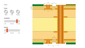
There are two types of microvias: buried and blind. Buried microvias are filled with conductive paste before being plated, while blind micro vias do not have any filler material and are simply drilled to a precise depth. Both types are then deposited and plated with copper. The plated interface between two stacked microvias or that between a blind microvia and a pad can fail due to thermal cycling. This happens because the plated surface of the microvia expands and exerts high stress on the thin copper, which eventually breaks down. This is why it’s important for designers to choose a low aspect ratio for their microvias – 0.7 or lower.
How Micro Vias Affect the Manufacturability of PCBs
Aside from the aspect ratio, another consideration is whether a PCB’s microvias are stacked or staggered. Stacked microvias align with one another layer to layer and resemble the structure of through-hole vias. Staggered microvias, on the other hand, are offset from each other by one or more layers and use traces to connect in the x- and y-plane between layer transitions. Staggered microvias can be useful when there is a need to spread out heat-generating components or other features on the PCB.
As a general rule, it is best to stagger microvias in vertically-stacked interconnects to reduce the risk of failure at the plated interface between the top surface of a stacked microvia and the bottom of its adjacent copper layer. Voiding also appears to be related to failure, but it depends on the shape and volume void fraction of the microvia, and the aspect ratio and void size of the via.
In addition to avoiding the pitfalls of stacked microvias, PCB manufacturers should ensure that they have a high-quality plating process for all microvias. This will help minimize the potential for voiding and copper concentration at the plated interfaces, as well as ensure that the copper wrap plating is of sufficient thickness to support the via body. Lastly, it is important to ensure that the laser used for drilling the microvias has the right wavelength to avoid excessive damage to the copper during the process.