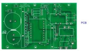
significance of the pcb and pcba layout
In the intricate world of electronics manufacturing, the layout of printed circuit boards (PCBs) and printed circuit board assemblies (PCBAs) holds profound significance, influencing every aspect of a device’s performance, reliability, and manufacturability. From optimizing signal integrity to enhancing thermal management and streamlining assembly processes, the layout plays a pivotal role in shaping the functionality and efficiency of electronic devices.
One of the foremost considerations in PCB and PCBA layout design is signal integrity. Signal integrity refers to the preservation of signal quality and fidelity as it traverses the circuitry. The layout of traces, components, and signal paths on the PCB directly impacts signal integrity, with factors such as trace length, routing topology, and impedance matching playing critical roles. By optimizing the layout to minimize signal reflections, crosstalk, and noise, designers can ensure reliable data transmission and optimal performance of the circuit.
Efficient thermal management is another crucial aspect influenced by pcb and pcba layout. Electronic components generate heat during operation, and inadequate heat dissipation can lead to thermal stress, premature component failure, and degraded performance. The layout of components, thermal vias, and heat sinks on the PCB directly affects heat dissipation capabilities. By strategically positioning components and thermal management features to optimize airflow and thermal conductivity, designers can mitigate thermal hotspots and ensure uniform temperature distribution throughout the board.
What is the significance of the pcb and pcba layout?
Moreover, the layout of PCBs and PCBAs significantly impacts the manufacturability and assembly process. Design for manufacturability (DFM) principles dictate that layouts should be optimized to minimize assembly complexity, reduce soldering defects, and facilitate automated assembly techniques such as surface mount technology (SMT). By clustering components with similar footprints, orienting components for easy access by pick-and-place machines, and adhering to assembly guidelines, designers can streamline the manufacturing process and minimize production costs while ensuring high-quality assembly.
In addition to technical considerations, the layout of PCBs and PCBAs also plays a crucial role in optimizing space utilization and form factor. Compact and densely packed layouts not only maximize the functionality of electronic devices but also reduce material costs and footprint, making them more cost-effective and portable. By carefully arranging components and traces to minimize wasted space and optimize routing efficiency, designers can achieve sleek and streamlined designs that meet the demands of modern consumer electronics.
Furthermore, the layout of PCBs and PCBAs impacts the overall reliability and robustness of electronic devices. Layout decisions such as trace routing, component placement, and grounding techniques directly influence factors such as electromagnetic interference (EMI), thermal stress, and mechanical stability. By implementing best practices in layout design and adhering to industry standards and guidelines, designers can enhance the durability and longevity of electronic devices, reducing the risk of premature failures and improving overall user satisfaction.
In conclusion, the significance of PCB and PCBA layout cannot be overstated in the realm of electronics manufacturing. From optimizing signal integrity and thermal management to streamlining assembly processes and enhancing reliability, the layout plays a pivotal role in shaping the performance, efficiency, and functionality of electronic devices. By leveraging advanced design tools and adhering to best practices in layout design, designers can unlock the full potential of PCB and PCBA layouts, delivering innovative solutions that meet the evolving demands of the electronics industry.